2 Big Players in GaN Market Face Off in Patent Dispute
As the demand for gallium nitride (GaN)-based devices grows, so does the chipmakers’ determination to protect their intellectual property rights. The recent patent dispute between Efficient Power Conversion (EPC) and Innoscience, two prominent players in the GaN market, demonstrates this.
GaN technology is revolutionizing power electronics applications. Its ability to operate at higher frequencies, handle higher power densities, and deliver superior performance makes it crucial for power electronics, wireless power transfer, 5G infrastructure, and electric vehicle charging systems. As a result, owning and protecting GaN patents provides a competitive advantage and the potential for significant market dominance.
On May 24, EPC announced that the company filed complaints in federal court and the U.S. International Trade Commission (ITC), asserting four patents of its foundational patent portfolio against Innoscience.
Founded in 2007, EPC has been at the forefront of GaN-based power conversion solutions. Headquartered in El Segundo, Calif., the company holds a robust portfolio of GaN-related patents and a strong industry reputation. EPC’s patents cover various aspects of GaN technology, including transistor design, manufacturing techniques and device integration.
EPC created the first commercial enhancement-mode GaN power devices, in 2010. As a fabless company, EPC uses foundry suppliers to produce GaN-based in large quantities. EPC has built a comprehensive IP portfolio that includes patents granted in China, Japan, Korea, Taiwan and the U.S.. This includes 57 U.S. patents and 172 patents elsewhere.
According to EPC’s complaint, Innoscience hired two former EPC employees and assigned them the roles of chief technology officer (CTO) and head of sales and marketing. Subsequently, according to EPC, Innoscience introduced to the market a series of products apparently identical to EPC’s products, claiming similar performance.
In addition, Innoscience recently claimed that many of its products have “pin-to-pin compatibility with existing products,” including those developed by EPC.
By suing Innoscience in federal court and the ITC for patent infringement, EPC is seeking damages. EPC also wants to stop Innoscience from importing infringing GaN products into the United States.
Headquartered in China, Innoscience is a relatively new player in the GaN landscape. Since its founding in 2015, the company has become the largest 8-inch, integrated device manufacturer only focused on GaN technology. The firm claims it produces 10,000 wpm (wafers per month) and continually increases its production capacity to reach and beyond 70,000 wpm.
Just two days after EPC’s announcement, Innoscience published on its site a response,, asserting that the four alleged infringements of fundamental GaN patents are without merit. It said it will pursue all legal options to defend itself.
Innoscience added that it has filed 753 patents globally, with 129 patents granted—and that claims of plagiarism based on the job changes of a few workers are unfounded. The company also states that its “intellectual property rights are clear, traceable and free from infringement.”
The patents in dispute, all filed by EPC in the U.S., are 8350294, 8404508, 9748347 and 10312335. These patents protect key design and production features of EPC’s exclusive enhancement-mode gallium nitride power semiconductor devices.
According to EPC, the patents cover developments that helped GaN-based power devices go from a research project to a high-volume, mass-producible substitute for silicon-based transistors and integrated circuits. GaN devices are more efficient, affordable and smaller than their silicon-based counterparts.
Granted in 2013, the 8350294 patent refers to the “compensated gate MISFET and method for fabricating the same.” The subject of the patent is the enhancement-mode GaN transistors. More specifically, it pertains to an e-mode GaN transistor with a semi-insulating GaN layer or compensating GaN layer above the barrier layer and below the gate contact.
Unlike conventional GaN transistors, which exhibit a high leakage current of the gate contact during the device conduction, the solution proposed with this patent (called MISFET) does not leak current during device conduction and is easier to manufacture. This is due to the introduction of the compensated GaN layer or the semi-insulating layer below the gate contact and above the barrier layer.
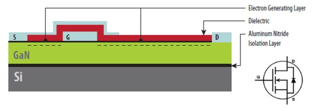
The structure of EPC’s GaN power transistor is shown in Figure 1. A thin Aluminum Nitride (AlN) layer is initially grown on silicon wafers to isolate the device structure from the substrate. A highly resistive GaN layer is then grown on top of this. A layer of Aluminum Gallium Nitride (AlGaN) is then applied to the GaN. The different materials, with different bandgaps, in the adjacent nitride layers contribute to forming a conductive two-dimensional electron gas (2DEG).

Figure 1: EPC’s GaN power transistor structure
Also granted in 2013, the 8404508 patent refers to the “enhancement-mode GaN HEMT device and method for fabricating the same.” Most nitride devices are typically ON (depletion mode devices) because the 2DEG area is present under the gate at zero gate bias. However, the device can become an enhancement mode if the 2DEG area is depleted (removed). Typically, the 2DEG region can be depleted by inserting a p-GaN or p-AlGaN layer between the gate and the AlGaN/GaN heterostructure.
Enhancement mode devices are often OFF and desired for the extra safety they offer and ease of operation using basic, inexpensive drive circuits. A positive bias must be placed at the gate of an enhancement-mode device for current to flow. A detailed method for obtaining an e-mode GaN transistor is the subject of this patent.
The other two patents, 9748347 and 10312335, refer to the “gate with self-aligned ledge(d) for enhancement-mode GaN transistors.” According to these patents, an architecture for reducing the gate leakage current includes a ledge beneath the metal gate with side surfaces that “extend horizontally” in the direction of the source and drain. A gate with self-aligned ledges has a significantly lower gate leakage current than conventional gates without ledges when the transistor device is in the ON state.
Next steps
An evidence hearing is set for February. And a decision on this dispute is expected in October next year. The legal proceedings will probably require significant time and financial resources. A sufficient budget for litigation is crucial, as the chances of success are significantly higher when working with a legal team experienced in GaN technology and devices.
At this moment, it’s difficult to anticipate the impact this controversy will have on the GaN market. However, if EPC prevails, Innoscience won’t be able to export its e-mode GaN HEMT devices to the U.S.
-
Previous:
-
Next:


